Contents
Thanks to Douglas Miller, the author of the Wang 700 simulator for sharing his wide knowledge about the intricacies of this machine, plus valuable reflections on the world of the engineers at the time. However, according to his wish, most of his comments through numerous e-mails, have been anonymously merged into my text, without much rewriting.
Intro

Fig.01 – The Wang 700 is still around, 1970 to 2023
This calculator or computer contains no microprocessor, the «program» is a state machine in a diode matrix, it has core for code and data, can do scientific calculations and is programmable. And it has nixie tubes. It’s from 1970 and it’s made in the US. It weighs around 18 kg. It is just beautiful engineering and computer science!
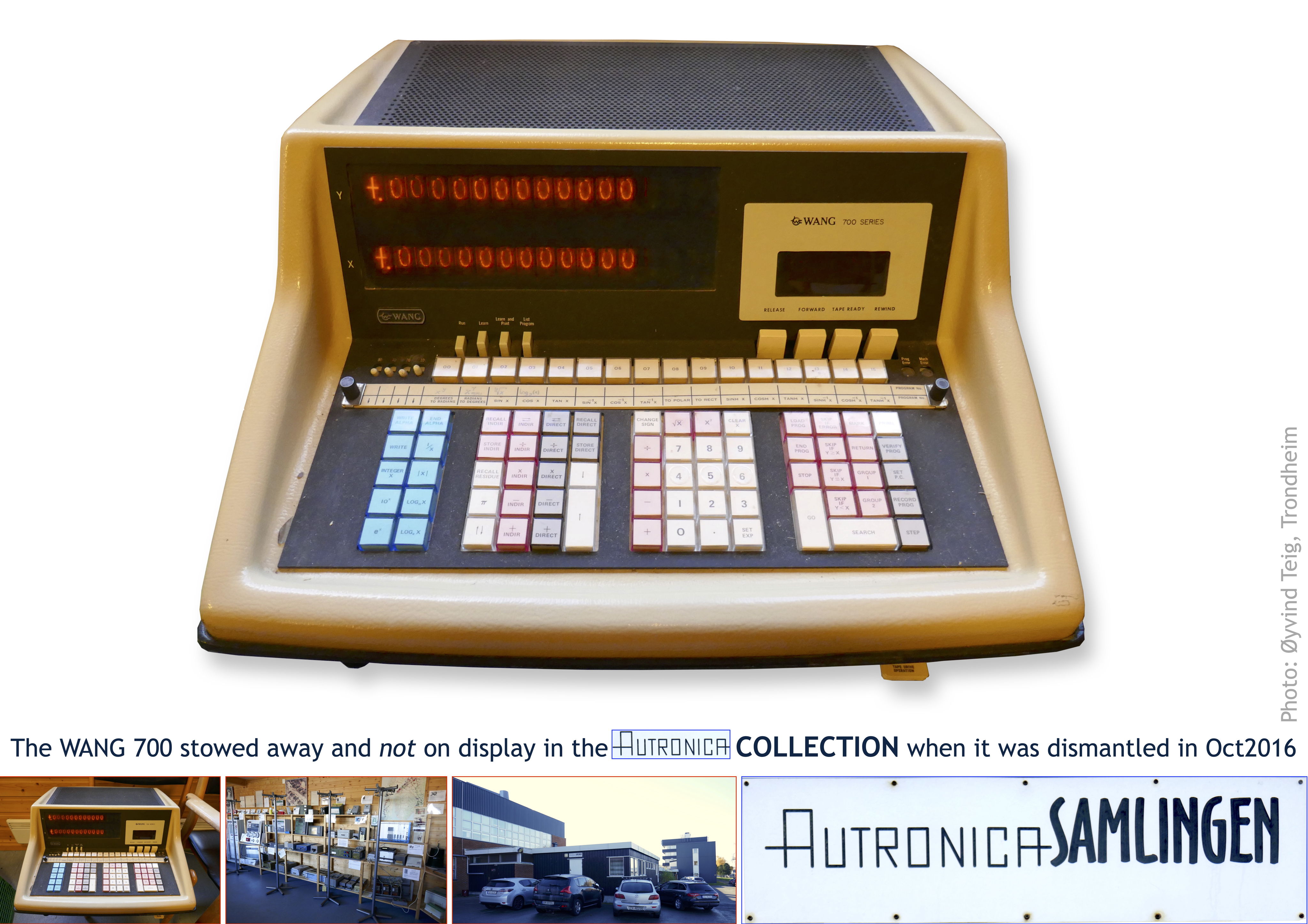
I have saved it from the trash container two times since it was taken out of use. First in 1985 when I brought it home, not 1982 as I first assumed. (I discovered the year in a copy of a hand written letter I had written to Wang, where I even got a reply. Stay tuned, I will publish them here. TODO) Then I gave it back to the newly started «Autronicasamlingen» (Autronica collection or museum), where it had a sordid position since it was no Autronica product. This was in the nineties. Then I saved it from the container again, when that collection was dismantled in 2016 (see Fig.03b). Some stuff went to Autronica Fire & Safety and some went to Kongsberg, since the original Autronica company had been split, just before the turn of the millennium. And some was ready for the container. But not this guy. It was ready to be brought home, again. And now, in 2023, it has been properly named «mine», so that I in fact can give it away.
Since I picked it from my cold loft and photographed it, I never powered it up. That’s why Fig.01 doesn’t show the nice nixie tube display.
Over there is back home

Fig.02
Before Christmas 2023 it will be On 15Nov2023 it became the property of an American computer museum! Status on the photo is as of 30Oct2023, where it’s awaiting the next level of packing. Previous colleague Morten S. at Autronica certainly helped me with that next level. Post in shop didn’t have a scale that matched, so they approved my digital handheld luggage hanging baggage scale’s value of «about 32 kg.», also probably rounded down by my memory. The package details, as seen on the net, was 33.8 kg, only 1.2 kg short of not being handled by Posten here in Norway. After it arrived I got this response: «All unpacked, excellent packing job, thank you! There is no damage. And what a beauty!». Yes, it is back home now!
The last rescuing

Fig.03b – The WANG 700 stowed away and not on display in the AUTRONICA COLLECTION when it was dismantled in Oct2016 (see Fig.03 here)
On the outside, this wasn’t my product. Well, the nice nixie tubes, the clicks and feeling of keyboard, cassette tape recorder and weight certainly attracted me. I mean, I never used it at job. I think it was mostly used to calculate transformers. Coil type, number of windings, type of iron and what do I know? These were formulae where a slide rule, seemingly, had lost its mission. The first microprocessor based calculators hadn’t arrived yet. And Autronica needed to calculate transformers since we used power supplies internally in our products, as well as developing and selling battery chargers. Even transductor motor driven regulators, for incandescent lighting at large cinemas, like the early Colosseum kino (movie theatre) in Oslo (here). I just assume that this calculator helped the engineers with all of this.
Maybe the new owners, who were also sent a pile of cassette tapes with programs on, perhaps some day may be able to tell more precisely.

Fig.04
For me, I had taken care of this computer for other purposes. I didn’t feel that something as nice as this machine should be thrown away. I must have felt this for more of the type. See photo of my cold (but dry) loft.
In 1985 (the year of my first salvation of the Wang) I hadn’t read the Turing book (Andrew Hodges: Alan Turing the Enigma) which I must have bought and read some years after its publishment 1983. I hadn’t been to Bletchley Park in 1996 and written about it in a Norwegian computer magazine (095:[3]). And there seen a Colossus machine being reborn. I wasn’t allowed to photograph it, but the man in charge said he’d take a walk. I hadn’t even been to Science Museum in London to absorb computer technology, from a Chinese Abacus via Babbage‘s Difference Engine to Ada Lovelace to the new then Personal Computer (PC) and on. But I did have a basic admiration of the stuff. After all, I had been in my rather cosy basement cave since I was a youth, or maybe even child; and I don’t know how many radio gems people presented to me – and I tore almost all apart to forever gone, and I arranged all the parts in numbered drawers and boxes. I still have some very old stuff on the same loft. Some about this in a note in Norwegian here: Radiobyggboken (Google translate there).
Disclaimer
Some of this stuff are assumptions on my behalf, or – between qualified and dubious guessing.
Some would be quoted from the 700A REFERENCE MANUAL, WANG LABORATORIES INC. 700-0251B 4-70 2.5M. Autronica had two, I kept the worn copy myself. It’s also at [1] – but a newer version is downloadable at [2].
If you find anything plain wrong, or even slightly wrong, or just have something you’d want to add, please comment below or mail me here.
Read-only memory (ROM)

Fig.05
At the bottom of the Wang 700 is a large diode matrix which implements a read-only memory (ROM) which functions as the control store of this machine. This store is accessed via address decoders. We can spot the wired connecting top side of it beneath the protective plastic in the above Fig.05 (lower part). (The trigonometric functions «are executed from the core memory» [1] page 1-1, which might indicate that constants like ℇ (≈2.71828) and π (≈3.14159) (Or Pi_3.14.. which I have consequently used in this note) are not in the diode matrix. I assume this also in general goes for all transcendental functions. They may even be nowhere, since they can be series expanded in subroutines).

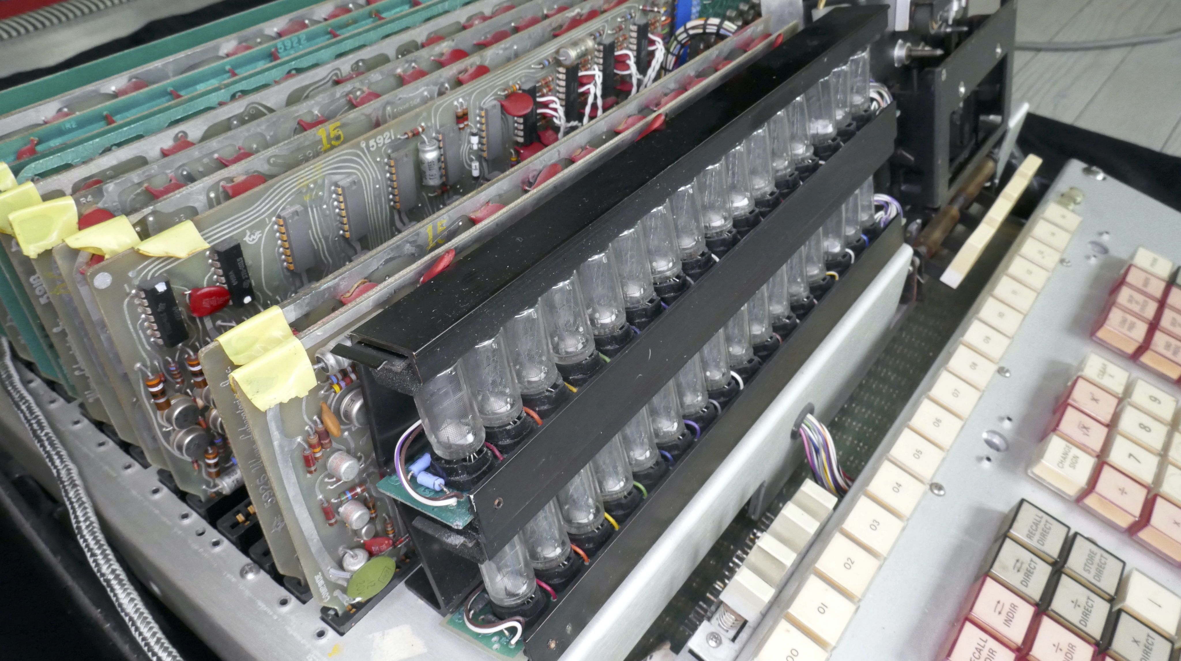
Fig.06 – Also see Fig.18
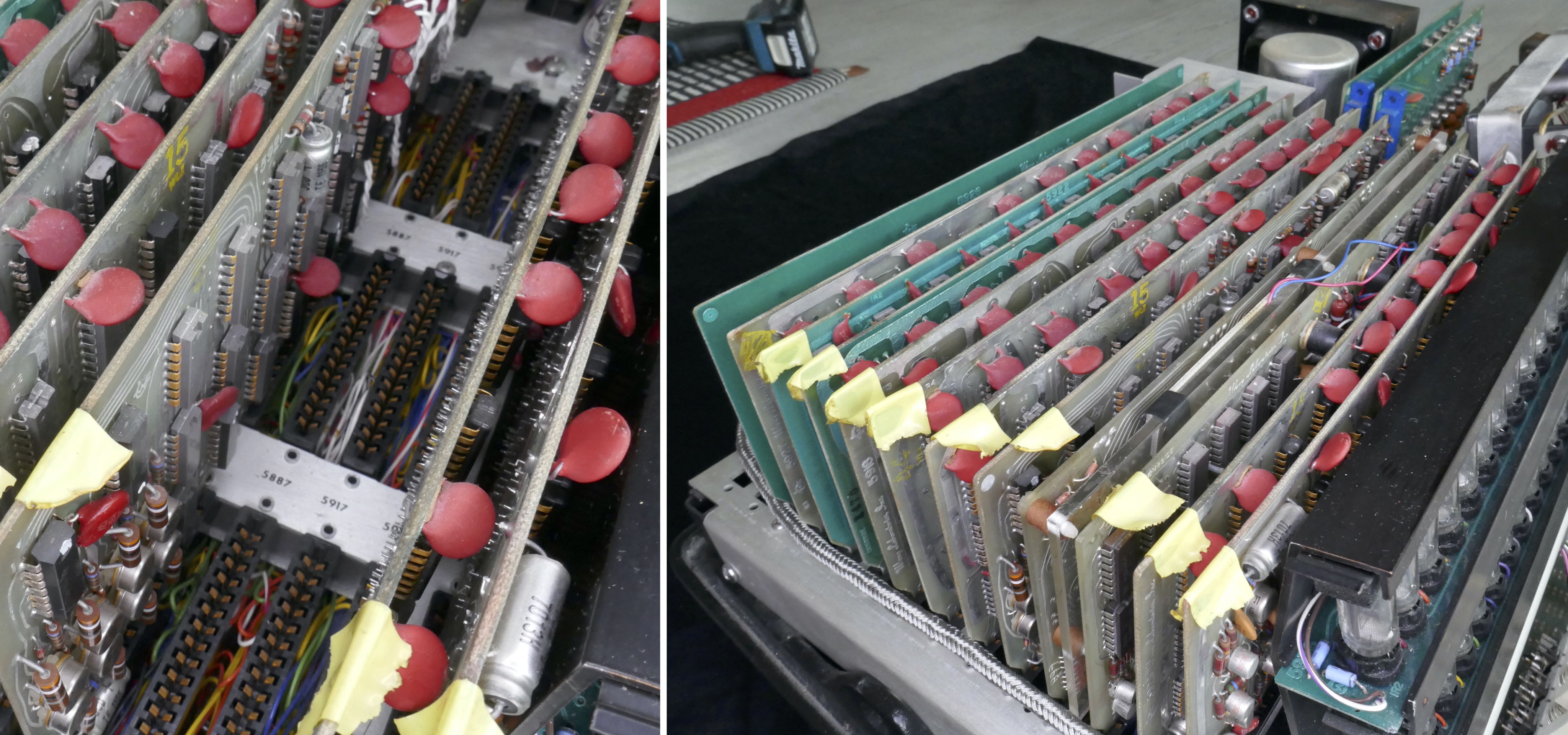
The above picture (as Fig.05) shows the wire wrap section. It connects all the plug-in circuit boards. We also see keyboard, plus (bottom) the top of the plastic protected diode matrix.

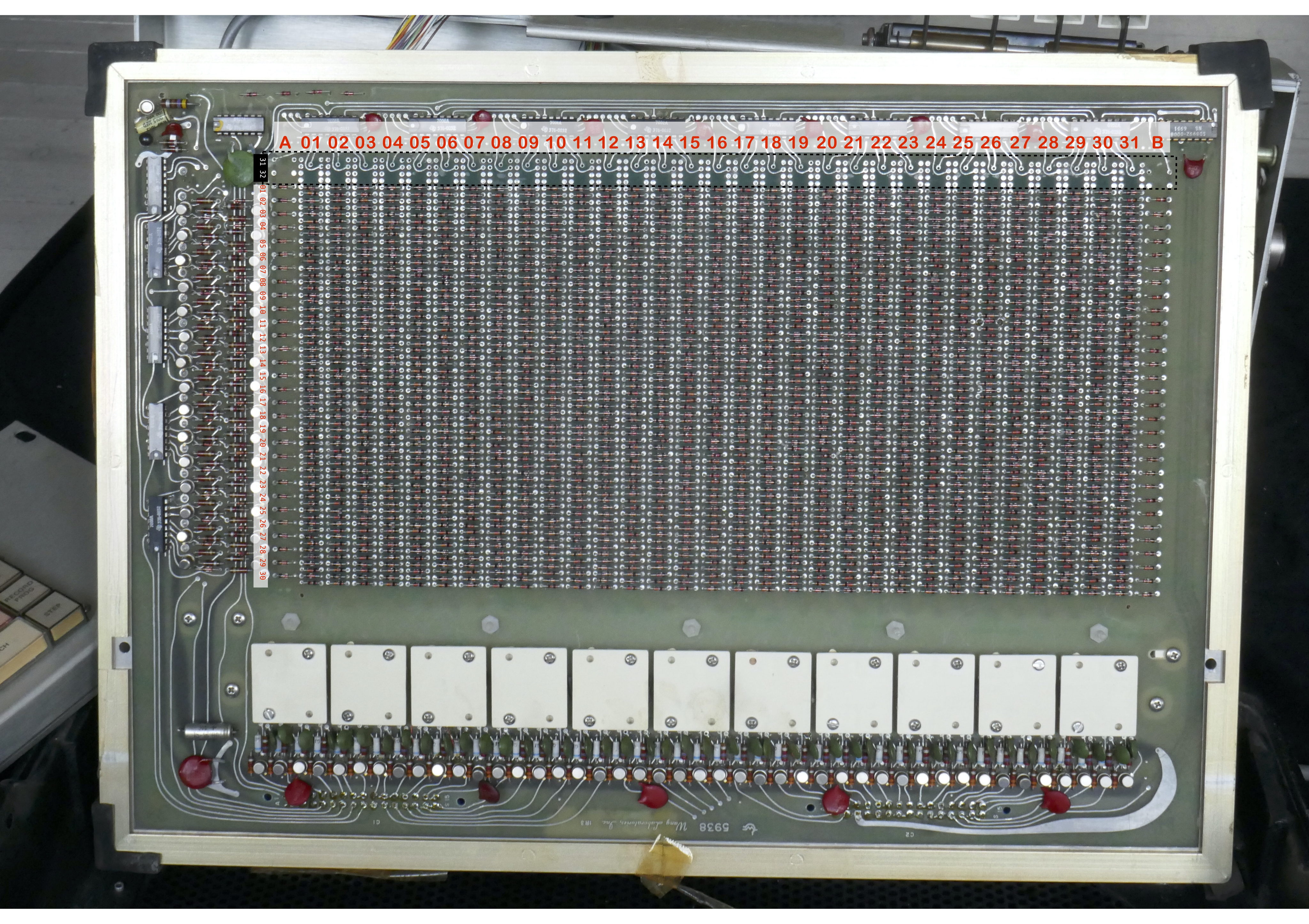
Fig.07 – 1920 diodes, eleven quad transformers (bottom view) and 44 transistors
Here we see the diode matrix. There are sights of it through the machine’s steel bottom ventilating holes. I have inserted rulers in this photo (now updated with empty slots count), so that I didn’t have to count them all. (There also are numbers on the wired side of the board, see below Fig.09). The number of diodes would be (30 * 2) for the left and right edges plus (60 * 31) for the central dense square, which would add up to 60 + 1860 = 1920 diodes. But the empty diode slots add to the description of the architecture. The unused positions, being (2 * 2) for the left and right edges plus (31 * 4) = 4 + 124 = 128. This means that the total possible address space is 1920 + 128 = 2048 words of microcode. To realise the needed functionality of the 700A, Koplow (below) needed at max 1920 microcode instructions. Now, what might the microcode word width count to?

Fig.12 – Four of the eleven quad transformers (top view) and wound wires. The diodes have common cathode or anode
At first I thought that each diode represented a bit of the microcode. However, for the microcode ROM, each of those ultra-thin wires represents one «word» of microcode (43 bits). There will be a maximum of 2048 of those wires, although locations that are not implemented will not have wires. Each bit of a word is determined by how that wire threads through those 11 quad-transformer assemblies, weaving in or out of each of the 44 transformers (only 43 used). When a current pulse is sent through one of the wires, each of those transformers is activated if the wire passes inside, and the resulting «1» is latched into external ICs. So, the diodes are actually used to ensure only one wire gets activated, since they are all connected as a matrix. There is one diode per wire (word of microcode), so there would be a maximum of 2048. The Wang 720C uses 2006 of the possible microcode locations, so I suspect it has 2006 diodes. The other models will have less microcode instructions and so less diodes. (See Circuit diagrams #17)
The diode plus transformer solution is called «wire weave» and was supposedly invented by An Wang. The wires are very thin (40 AWG (0.0799 mm)?) and fragile and would of course not take a lot of current. I was scared when I photographed.

The model is seen in this Fig.12.
Wang Laboratories, Inc.
ELECTRONIC SYSTEMS AND DEVICES
220V 50 HZ 75W
MODEL NO. 700A
SERIAL NO. 810763
TEWKSBURY, MASS. U.S.A.
The microcode for these machines is certainly mind-bending. The 700 «CPU» is a bit more primitive (than the 600), not having a stack or «call» instructions, but it was oriented towards core memory, which requires you to write after read because reading is destructive. Basically, there are bit-fields within those 43-bit words that control various encoders/decoders, channeling data to/from various registers (and also activating functions of the ALU). But there is a large bit field that represents the next microcode address to run. The CPU has no Program Counter or anything that advances automatically. The next instruction executed must be in the address field of the previous instruction executed. Part of the address field is used for conditional branching, the low two address bits being derived from a pair of decoders that select various status bits or constants. This makes the microcode listing very difficult to read, as it is rare that two adjacent instructions are actually executed in order.
The below (paragraph) is my early pondering over things. However, search for ‘mantissa’ in the text to read some more. Black box exploration may soon go wrong, even if sounds rather ok if this guessing would have been the end of story:
(Anyway I think it’s much smaller than the the internal data representation, which would most probably be binary, which would be floatN, with N somewhere between float32 (32 bits available for 7 decimal digits plus exponent) and float64 (64 bits available for 15-17 decimal digits plus exponent). Including a sign bit for both the mantissa and the exponent. However, the display reflects two of the 122 ferrite core registers [1]. The display itself has 12 digits + 2 digits for the exponent and I guess, one bit for each of those for sign. If per digit representation, one digit is 4 bits and a data word bit width is 4 * 14 = 56 bits plus 2 bits for signs = 58 bits. But there may be a binary-in-register (floatN) to binary-coded decimal (BCD) for the display functionality in one of the boards. Another complexity here is that the Wang 700 has a RECALL RESIDUE function, «a unique Wang feature that makes double-precision arithmetic a simple operation on the 700.» [1] page 1-1. I assume that the 12 digits of the display already shows double precision. We’ll come back to this, because it’s more related to the the display and the ferrite core.)

Fig.08
The chip «7008A» from Texas Instruments («TI») probably is a date code (8th week of 1970), and the part number is 376-0032 – which is a Wang part number (Even today, IC manufacturers will print custom part numbers on chips for big customers). The schematic for the ROM board says this part is 7445/74145 (although it quotes 376-0069). While those are decimal decoders, they actually use them as octal (binary) decoders – since the «8» and «9» outputs are not connected the «D» input is effectively an enable. So, they are decoding the address lines 3 at a time.» (Search for «schematic» here.)
I am quite certain that they did not have automatic placement of components in 1970. Nor that they came on a roll. In other words, they mounted by hand, every other one the same direction, and the others the other direction.
For the machine to work correctly with all instructions today, all these diodes have to work. These are glass encapsulated diodes which would have to have survived for 53 years. They don’t have their type printed on them, but they are obviously small signal diodes.

Fig.09
From the Wikipedia Diode matrix article (below) I quote: «A person would microprogram the control store on such early computers by manually attaching diodes to selected intersections of the word lines and bit lines. In schematic diagrams, the word lines are usually horizontal, and the bit lines are usually vertical.» In the above Fig.09 we see the connecting wires between these intersections.
Hand mounting the diodes is one thing, hand soldering these wires just adds to the admirable work needed – and the artwork thus presented. After 53 years some small and accurate hands deliver. I think about these people. I was 20 at the time, and I have no problem going back there. I can even feel the warm summer air towards my skin. Back then, it was now. These also were people of blood, and I guess, tears.
1970 and before were times when service manuals were half of the job (well..). I have some of those, even with hand drawn 3D perspectives. Like in the service manual of the 1959 Philips 17 TN 250A (17TN250A), as seen in the above Fig.04 (also mentioned in blog note 100). There were no flat component assemblies; everything was soldered in a chassis, mostly between tube sockets. True 3D. But any Wang 700 service manual probably might do with 2D. I wonder if there, any place in the world, might be a service manual for the Wang 700?
I think that the inductances seen would increase the speed, to avoid ringing on the lines, to balance out the reactive components of the transmission lines. I have not had the Wang open and scoped while it was at work, so I have no idea of the speed here. Maybe the new owners might have this secret revealed.
Now, look at the wires. One type of varnished enamelled copper wire is from 1916 (I found this ref.: «History and Future Prospects of Magnet Wire Development», Sugawara e.al. here). But I think they used oiled cotton tape to insulate the wires when my father wound power station generators around 1938-1945 (203:[A private aside]). These wires on the Wang are as jewelish as they look! Not one short is accepted! Not one, even after they all have been bent, twisted, de-insulated and soldered by some tiny hands.
Aside: the above Fig.09 is, as the rest of the Wang 700 photos here, shot with a Panasonic Lumix DMC-TZ100 camera on our living room floor, with a tripod. I did use a circular LED lamp to avoid too much shadows. The others are produced from the best JPG files it produces. However, Fig.09 is made in macOS Pages with two raw files as the source.
About the Wang 700
From the Wang Laboratories Wikipedia page [4] (18Nov2023) I read that:
(Intro) «Wang Laboratories was a US computer company founded in 1951 by An Wang and G. Y. Chu.[1] The company was successively headquartered in Cambridge, Massachusetts (1954–1963), Tewksbury, Massachusetts (1963–1976), and finally in Lowell, Massachusetts (1976–1997). At its peak in the 1980s, Wang Laboratories had annual revenues of US$3 billion and employed over 33,000 people.»
(Calculators) «From 1965 to about 1971, Wang was a well-regarded calculator company. The dollar price of Wang calculators was in the mid-four-figures. They used Nixie tube readouts, performed transcendental functions, had varying degrees of programmability, and used magnetic core memory. .. In 1971, Wang believed that calculators would become unprofitable low-margin commodities and decided to leave the calculator business within a few years.»
(The Wang 1200) «Harold Koplow, who had written the microcode for the Wang 700 and its derivative the Wang 500 rewrote the microcode to perform word processing functions instead of numerical calculations.»
The WANG MUSEUM by Jan van de Veen in the Netherlands also has a Wang 700, plus lots of pictures and stories [3]. It also has some quite interesting facts about the 700:
«In December, 1968, WANG Labs announced the new 700-series calculator to compete directly with HP’s 9100 calculators. As many people who know high-tech industry understand, the announcement of a product doesn’t necessarily mean it exists. Even back in late 1968, the notion of “vaporware” existed, and WANG’s introduction of the 700-series was just that. Even though the product had been announced, shipments weren’t promised to begin until mid-1969, which, as it turned out, was a milestone that WANG missed by a few months. In February of 1969, McGraw-Hill Publishing’s Product Engineering magazine published a cover-story on the new (and not yet available) WANG 700, featuring a proud, cigar-toting Dr. Wang surrounded by a number of 300-series keyboard/display units and his new baby, a prototype WANG 700. Cooling was a problem, but soon a fan was introduced that solved the problem.«
Also worth reading is the The Old Calculator Museum‘s pages, see [5].
Then the book Lessons: An Autobiography, by An Wang, see [8]. I don’t know how much the Wang 700 is covered. However, this text is from Amazon (here): Book Description: «This story of the man behind Wang Labs offers lessons about building a company, including managing growth in moderation, keeping the spark of innovation alive in a huge corporation, and standing up to an agressive (sic) competitor.» From Publishers Weekly: «One of the 12 recipients of the Medal of Liberty awarded this year to distinguished naturalized citizens, Wang started the electronics laboratories that bear his name as a one-man shop six years after his arrival in 1945 from China at age 25 and built it into a multinational company. In this forthright autobiography, ably assisted by Linden (Silent Partners, etc.), he attributes his success to adapting technology to society’s needs and applying to his business practices Confucian values of balance, moderation and simplicity. Surviving the upheavals in China of the ’20s and ’30s and the Japanese invasion of the ’40s, in which he lost his parents and a sister, Wang came to the U.S. as an industrial apprentice. After earning a doctorate in applied physics at Harvard, through his research he achieved a breakthrough in computer core memory design. The cores he manufactured would make him a rich man, as did business and general purpose computers and word processors developed as compatible systems. In his memoir, Wang, a dedicated philanthropist, shows that ethical standards areas vital to him as commercial success. Copyright 1986 Reed Business Information, Inc.» Update 23Jan2024: I have now received this book. It contains a chapter on the invention of the magnetic core, plus several pages on the development of the 700. Very interesting reading. It’s from 1986, so I assume I could scan some of the pages and publish them here. But I’ll check with the publisher’s first (TODO). A value-added add-on for me is that the book has been signed on the cover page by An Wang. (In addition to that autograph I also have some other autographs from notorious computer science people, see Wikipedia).
Not wire wrap

Fig.10 – Not wire wrap, by a closer look
This wiring is not of the sort wire wrap. (The term is not not even relevant, so I haven’t included it in the Wiki-refs list below.) Wang must have needed thicker wires than the 30-28 AWG, which would have been required for wire wrap. And the posts would have needed to have a square profile and be gold plated, so that the silver-plated wire coating could have properly cold-welded to the golden posts, to produce the mega solid connection that wire wrap technology gives.
Wang have used some kind of connector that seems to be clamped onto their silver-plated(?) posts. Probably also mega solid. I have no clue what this is called. I assume that the cables’ insulation is PVC 196:[My materials science notes]. I love the material, but I’m not certain if I should..
The wire wrapped backplane is not very bus-like. If it had been they probably wouldn’t have wire wrapped it, but designed a back-plane board. Even if the 700 has one board for «A-Bus» and one for «B-Bus». Our model had 1k * 8 core. On a model with 2k core, the #3 and #4 boards would be replaced with 5929 and 6038 to upgrade the memory. Although, it appears that the backplane wiring would also need some changes, as well as the microcode. If we study the price sheets, we’ll see that the cost of the upgrade of a machine is significantly higher than the difference in price between the same models. Seems like, in almost all cases, it was never a simple matter of replacing boards in slots, but it required a more-invasive approach. It might have been the case that field techs mostly just swapped the whole machine, and then did any alteration to the original back at the factory (and used it for another customer’s upgrade).

Fig.18 – The numbering of the boards is also seen (detail of Fig.06)
In the figure above we again see the whole of the bottom. The numbering of the boards is easier seen than in Fig.06. It goes from front as #1 to rear as #12 with two extra empty slots in the back. If this is the numbering of the connector positions only, since it’s printed in the bottom – and not numbering of the boards as such, I have later nevertheless used the same numbering scheme for the boards proper.
The transformer’s board is also seen, as well as part of the tape deck.
My orig photo had some perspective that I removed with Photoshop Elements, but then I needed to fix the x/y ratio. I have done this by assumption, don’t measure its ration from this photo!
The keyboard and its printed circuit

Fig.11 – The keyboard’s printed circuit from below (lower of picture is closest to the display)
This board is hand soldered, you can see this from the fact that only the through-holes are soldered.
This printed circuit board would be an example of hand made etched traces technique. However, not hand drawn as such, but as «the sweeping curves in the traces are evidence of freehand design using adhesive tape» (Wikimedia photo here). I remember these rolls of thin, black tape, in some kind of a dispenser, to be applied carefully so that it didn’t break – as that would cause broken wires by conception to appear on all the etched boards. Obviously the copper is etched away for all of the surface, but not the area covered with tape. So a successful wire better be made with a continuous tape. (Aside: when I was a youth I «borrowed» my mother’s nail polish bottle, containing that nice brush, to paint the wires. Then I think I used ferric chloride (Iron(III) chloride) that I bought a the local pharmacy to etch away the copper.
The above is about making one of a board. I don’t know how they produced thousands, but I think the technology of using photosensitive material and UV light was available at the time.
The four keys just below the display («Run», «Learn», «Learn and Print» and «List program») are mounted on the keyboard’s metal frame. The cables on the short side are the wires to the key (matrix?) I think. The extra, rather thick cable, goes to some output connector. This looks like a true add-on, mounted in the rear of the machine, «in the air» between the TYPEWRITER and the I/O connectors.
About the keyboard from the top. They might be micro switches, because they feel and sound expensive.
Memories from the users
Autronica
Wang 700
In November 2023 I spoke with the also retired colleague Harald Bjerkan (*1) about his memories of the Wang 700 and how Autronica produced printed circuit boards in the early ‘seventies.
Bjerkan, along with the technical director Bjørn Rennemo (*2) visited a shop or a demo room at Nordre gate here in Trondheim some time in 1970. (I checked the labels and stamps on the accompanying documents, and the demo they visited may have been by the company Gallus-Plesner AS; which Bjerkan also thought plausible. The machine’s production year was 1970, and it’s not likely that it would have been for sale for too many months or years. We might be talking about 1970 or 1971 for the year when Rennemo and Bjerkan visited that shop and the rather immediate purchase.)
The first usage of the 700 was to calculate the Fresnel lens of a buoy (Autronica LE-4). It was rather large, and had three incandescent lamps and a rather large battery, and electronics and a mechanism to rotate to the next lamp when one was broken. They developed a usable formula for a lens of of polycarbonate, with its refractive index. It was based on curves built up by straight lines. In the late fifties Autronica had been established to develop and produce fire detection (BS-1). But also small flashing lights for road work, with a much smaller Fresnel lens (LB-3). I remember these from when I was a boy. They were already then spread over the whole country. We used to place our mittens over them and have a look inside, to see that it started to blink in the newly established, mystic dark. The Rennemo and Bjerkan program for the Wang printed out a table which the designer (Oddvar Lyngstad (*3)) at the drawing board used, together with an HP-25 calculator to do the rest of the calculations. This must have been in or after 1975. I sense here that the HP-25 must have been a late, but good comer in the game. This finished the model that was used for moulding the Fresnel lenses. About 10 000 of these were produced. (By the way, I think I have the remains of exactly that HP-25. Stay tuned)
Bjerkan confirms that the Wang 700 also was used for for transformer design. This was mostly done by Asbjørn Tokstad (*4). He also printed out a table with data for each transformer design.
Autronica had also bought a modified IBM Selectric type writer, which was the «printer«. They had different typing elements or «heads» to choose from, making it possible to change fonts or character sets. (Using a Norwegian type head (with Æ, Ø and Å) it was also used as an off-line, manual type writer, Bjerkan tells.) I don’t know where the Selectric was connected, but probably to the original TYPEWRITER connector. But I do remember that I had the choice in 1985, to also bring the Selectric and the cable home. Unfortunately I did not.
Bjerkan also told that when they saw the Wang demonstrated here in Trondheim, the people there had made a program where they moved something from the «left» and the «right registers», «further or less up on the stack». When that program was ran, they heard this music score on a the long wave of a listening AM radio. I told about this in a mail to a guy at the museum and here’s a quote from the reply: «it’s a good illustration of why (at least in the US) the FCC had stringent requirements for EM interference, and the early home computers were clad with very costly metal shielding».
Additional sources:
[A1997]: .. «og livet går videre«. En beretning om Autronica gjennom 40 år. («..and life goes on». An account of Autronica over 40 years.) By Harry Amundsen (1997)Printed circuit boards
Harald Bjerkan also helped with explaining how Autronica produced their printed circuit boards (PCB). The general impression is that at this time this was no kitchen table work. They had quite a lot of machines. He sent me some pictures, I may come back with this, if any points towards PCB production.
At the start they bought copper-covered boards (substrates), but the wires were outlined with a sharp knife. Then the copper in the land in between was torn away. No etching at all.
Then Fritz Borgan (*5) worked with setting up more professional board production facilities. The basic principles were that the copper-covered substrates also came with a photoresist layer. (I will keep on naïvely trying to describe the process here, but the Wikipedia Photoresist article is a much better read, from which I think that the photoresist Autronica used was of the negative type.) A negative film (where the wire land was transparent) was made from a positive component layout with black wires. The negative was placed on the photoresist. When light was applied, the photoresist got some quality where the wires should be, this quality made the wires become hardened when soaked in a developer. Then the board was placed in a bath with iron chloride (Bjerkan thinks), which etched away the not hardened copper fields, but not the hardened wires. Then the photoresist was washed away, so that the copper became solderable. After this only the holes needed to be drilled. This was the basic mechanism that the machines did around 1970. Bjerkan is uncertain about whether at this time Autroncia had this production done in-house or out of house.
I assume that the Wang boards must also have been produced with this same basic technology.
Persons
(*1) Harald Bjerkan was a development engineer (the third hired), construction manager, quality manager, factory manager (86 in 2023)
(*2) Bjørn Rennemo was a technical director at the time, also one-of-four cofounders and co-owner of Autronica. I have also mentioned him in earlier blog notes
(*3) Oddvar Lyngstad was a mechanical design engineer, and also the head of the mechanical design department
(*4) Asbjørn Tokstad was a senior development engineer, in charge of power supplies and chargers etc. See 209:[Autronica SC-1]
(*5) Fritz Borgan was a manager in the production, and had been the first development engineer at Autronica
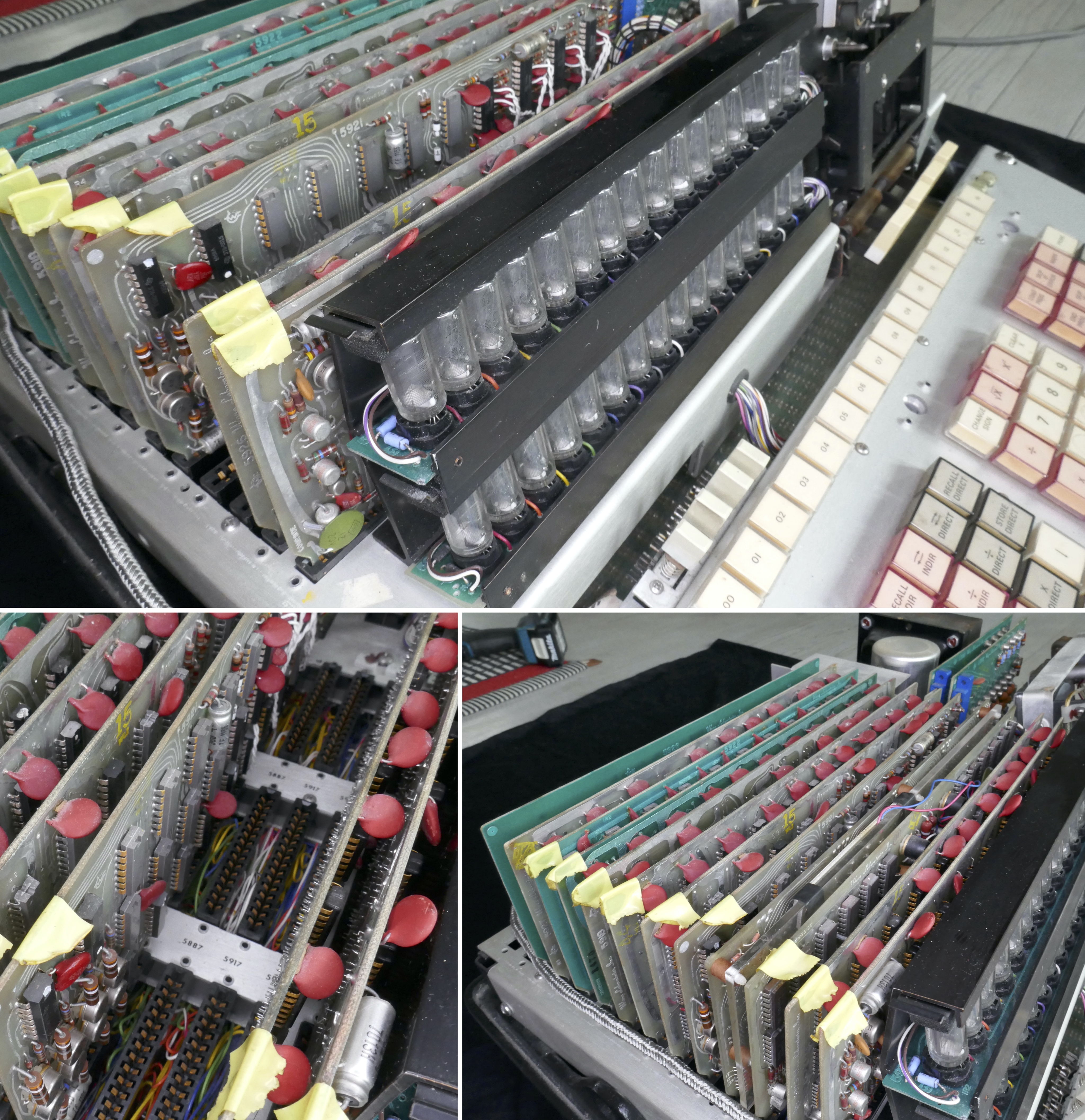
The core

Fig.14 The core. 32×32 bits x 8 = 8192 bits
The below photo shows a mesh of 16 individual cores in a 4 x 4 grid. There are four wires through each toroid. See Wikipedia (here) for a detailed description. There is one board in the Wang 700, counting up 8 fields of 32 x 32 toroids, giving the user 8192 bits of non-volatile memory. This time a toroid indeed is a bit; no complicating transformers to relate to.
Even if the memory retains its contents after the machine has been switched off and on again (provided there was not a single glitch pulse to mess this up), its main function is as the working memory, where intermediate values are stored.

Fig.15 – 4 x 4 toroids are 16 bits
(Thinking about it, maybe I should have rigged my camera better, to shoot a real close-up, for these toroids are small. One to half a mm diameter? But I didn’t want to touch any of these hairy wires, after all I was going to give it away, not tear it up. Placing a very close tripod by the board I considered too risky, but rethinking – it should have been ok. After all, the board was loose from the rest of the machine.)
In my Beep-BRRR project I use a FRAM (FeRAM) chip (ferroelectric RAM, random access memory) to easily store values which need to be retained after a power cycle. These cores on the Wang would function much the same way. Neither FRAM nor core would wear by being used, as opposed to flash memory, replacing rotating disks in modern computers.
The core memory organization is also interesting. The core RAM is organized in 8-bit «words», which are used directly for program steps but for data they are split such that the high 4 bits are for one register and the low 4 bits for the next register. This makes refreshing the display easy, as both X and Y are refreshed in the same cycle. But it does make it more difficult for programmers planning on how to use memory for registers. The 600 simplified this a lot for programmers, and of course has only one display register. The 600 also used semiconductor RAM so didn’t have the issues one has with core. The 700 core RAM was not reliable during power off/on, so you could not depend on it retaining the contents after a power cycle.

Fig.17 – Boards 3 (bottom) and 4
Here we see the core board (top, #4 according to the numbering in the next chapter) and its plastic protection. This is screwed onto that board, but a small piggy backed board with some diodes are placed on the protective plastic – with wires to the other board – board #3 (bottom). On #4 we see the top side, facing #3’s bottom side.
It looks and feels like a prototype, and not serial production. I had to unplug both board #3 and #4 to photograph the cores on board #4 since they were that intricately twinned.
But I learned that it’s not a prototype trait.
That odd «add on» to the core memory and core drivers boards. Those «out board» diodes are a thermal sensor and they are used to either protect the memory from over heating or (more likely) provide thermal feedback to auto-adjust the current driving the cores. You can see the diodes on the 5917 schematic in the lower-left corner, in a box labeled «P.C. 6085». Studying the schematic (TODO) will in fact reveal which of those alternatives is correct.
There are stories from people that worked on mainframe computers of the 60’s talking about what it took to get core memory to run (and keep running reliably). Introducing a new bank of core memory sounds like an arduous process that may have a taken many long days trying to calibrate it all.There is a 100-ohm potentiometer on the 5917, which probably was for that sort of calibration. By 1970 «the industry» had worked out some pretty good «best practices» for core memory… just in time for semiconductor RAM to make it all obsolete.
It seems that An Wang was one one the inventors of the core. From [10]:
«In the early fifties, An Wang had worked with the IBM company and contributed to the invention of the magnetic core memory there. He did not feel that his work was appreciated enough and he so founded his own computer company aiming to dirve (sic) his former employer out of the market.«
Bird’s eye view of the boards

Fig.16 – Bird’s eye view of the boards
You may see other versions of the above pictures here and here and here.
The block diagram from Miller’s simulator is included below. However figuring out what maps to which board isn’t really possible from that info. It’s a functional block diagram, intended to understand the microcode, not to map the boards.
Board #1 is the board just behind the display. Also see Fig.18 (above). I didn’t find any clue in my photos about the board types of #1, #7 and #9, neither in the photos here or in those I haven’t published, and especially not in those I alas did not shoot. Therefore, matching type and position have been guessed or inferred for these three. Also on fine studying of [11], which seems to confirm the red choices. Also [12] which even has photos of all the boards! The bottom of the table is the front, meaning that we view that boards from the top, as opposed to Fig.18, which is from underneath.
| # | P/N |
Wang title | Description |
| Schematics | |||
| #12 | 5928 | BUFFER BOARD | Drivers for signals requiring more current, mostly I/O related |
| #11 | 5927 | GENERAL I/O | Implementation of GIOA, GIOB registers and most peripheral control signals. Latching of keyboard special function keys |
| #10 | 5922 | ROM DECODER | Latches microcode instruction and decodes operand fields (excludes JH, JL, JAD) |
| #9 | 5923 | JH, JL, JAD (ROM ADDRESS) | Latches JH, JL, JAD and generates next address |
| #8 | 5918 | ALU | 4-bit BCD / Binary Arithmetic-Logic Unit |
| #7 | 5920 | BUS-2 | Implements S, T, U, V registers and corresponding part of A-Bus |
| #6 | 5919 | BUS-1 | Implements A-Bus and B-Bus |
| #5 | 5921 | SENCE (*) AMP. OSC COREBIT DRIVE | Implements RA, RB registers and analog interface to core memory. Also implements main system timing clock |
| #4 | 5887 | MEMORY CORE 32 x 32 x 8 | 1k x 8 core memory array, physically organized (addressed) as 32 x 32 x 8 = 8192 bits. Photo Fig.17 (top) |
| #Δ | Plastic protection++ | Five diodes for temperature sensing of the core. Screwed onto board #4, but wires go to board #3. Photo and text by Fig.17 (bottom, only plastic there) | |
| #3 | 5917 | X & Y CORE DRIVER | High-current drivers for core memory, with decoders for L, M, N registers (core address). See Fig.17 (bottom) |
| #2 | 5926 | KBD, CORE ADDRESS, KEYBOARD REG. | Implements KA, KB registers with I/O Port input override. Digital Tape Data interface. Implements L, M, N registers (core memory address). Only bits 0, 1 of L are implemented (1024 x 8 core memory) |
| #1 | 5924 | TAPE IN & OUT, NIXIE TUBE DECODER | Analog interface to tape read / write head. Refresh decoders for X and Y displays |
(*) sic (I don’t think this spelling makes sence sense, but it’s taken from the circuit diagram).
The diagrams, an overview below. Just press to get the PDFs (The layout managers of different browsers may render them not equal, even if they are in the html.)
 |
 |
 |
 |
| #1 5924_tape_display | #2 5926_kbd_ramadr | #3 5917_logibloc_X_Y_core_driver | #4 5887_1A_logibloc_memory_ core_32x32x8 |
 |
 |
 |
 |
| #5 5921_700_720_timing | #6 5919_bus1 | #7 5920_bus2 | #8 5918_alu |
 |
 |
 |
 |
| #9 5923_700_rom_next | #10 5922_rom_decode | #11 5927_gen_io | #12 5928_io_buf |
Then there are two other boards plugged into the chassis:
| #A | L505X | Higher voltage drivers of the Nixie tubes | Situated by the transformer, closest to the tape drive |
| #B | L505Y | Higher voltage drivers of the Nixie tubes | Situated by the transformer, closest to the transformer |
Diagrams here:
 |
 |
| #A 5945_X_700_logibloc_x_nixie_ control_anode_switch |
#B 5945_Y_700_logibloc_Y_nixie_ control_anode_switch |
Those L505X/L505Y slots correspond to schematics 5945-X.pdf and 5945-Y.pdf. They are the (higher voltage) drivers of the Nixie tubes. Both of those schematics seem to be functionally identical, the only difference being what connects to «J1» (either the «X» or «Y» Nixie tubes) and there appears to be difference in the slot wiring, where the «BL» (blink, i.e. flash) signal is not connected to the display slot for «Y». This «BL» signal is probably unconnected on the backplane, so that the «L505» boards are then truly interchangeable. So it would be that 5924 drives both L505X and L505Y, which each (respectively) drive Display X and Display Y Nixie tubes.

The Wang 700 block diagram (Courtesy of Douglas Miller). «In the above diagram, fine lines represent single-bit (and serial) data paths, while thicker lines represent multiple bits of data in parallel (typically 4). Note, the hardware implements both parallel and serial paths, depending on registers and access operations.»
(The original of the diagram is a gif file, but WordPress scaling seemed to cause thin lines to disappear. That’s why I use a jpg file instead.)
Here are some Miller quotes that I think best not anonymised into the text, since they are too detailed for me to have dreamt up:
Numbers are represented as floating point BCD values, using 16 4-bit «nibbles». The first nibble is the sign for the mantissa, the next 12 are the mantissa digits, next is the sign for the exponent, and the last two are the exponent digits. While normally the digits are BCD (0-9) and the signs are 0/1, it is possible to store any values in memory and then RECALL them to use as numbers. These numbers do get «normalized» promptly, usually after the first calculation. However, I did use this «feature» on the 600 to make animated displays of shifting «0»s, and also to be able to make the display truly blank. The 700 uses a different scheme to display numbers, and I did not work on trying to do similar tricks there. Because the 700 uses 16 program steps to store two numbers, it is a bit more difficult to read a number value by looking at the program memory – but it is possible. The mantissa sign is stored in the lowest numbered program step of a register pair, and the high 4 bits of the steps contain «register+0» while the low 4 bits contain «register+1»
Also, perhaps disappointingly, things like the constant Pi_3.14.. are simply stored as a string of digits, in a manner of speaking. Looking at a trace of the «π» key, you can see each digit being entered into the memory for display X… 3 1 4 1 5 9 2 6 5 3 5 9. Since Pi is a «normalized» floating point number already, the exponent is just left as 00 (implied decimal point after the first mantissa digit). It’s actually rather ingenious, because the microcode can only conditionally jump to one of four addresses and each digit entry must be a separate microcode instruction (address). They’re able to re-use a surprising number of instructions – considering. The Wang 600 was much more efficient, having microcode «subroutines» (but a rather shallow stack).
I’ve heard that Wang used some sort of «compiler» to make the microcode (there is evidence in the microcode itself), but I don’t know what sort of mainframe or minicomputer they compiled it on – possibly even renting time from someone else. I suspect, but can’t confirm, that they also used some form of simulation in order to test their microcode – the cost (pain) of debugging on a real 700 would have been huge – although it is possible that they had some sort of «development rig» with a special microcode store that was read-write (or at least easily modified). All conjecture, though. Back then, PROM / EPROM / FLASH were fantasy, so it would have had to been either core memory with a special hook-up, or something like magnetic drum (with considerable «fetch» latency). Or something I can’t imagine.
Circuit diagrams
Some individual schematics are included in the tables of the above chapter (12 + 2 = 14). Just press the board type names. There are some more diagrams as well (6), starting at 15:
- board_NN_wang_700_5936_display.pdf
- board_NN_wang_700_5937_keyboard.pdf
- board_NN_wang_700_5938_rom.pdf – See [11,E] there: «A total of 44 trans.«. These are the transformers shown in Fig.12. (By the way, I don’t know why this diagram is not in the top 12 list, expanding the list to 13)
- board_NN_wang_700_5945_disp_decode.pdf
- board_NN_wang_700_5975_gen_io.pdf
- board_NN_wang_700_5976_io_buf.pdf
 |
 |
 |
| #15 5936_display | #16 5937_keyboard | #17 5938_rom («44 trans.«) |
 |
 |
 |
| #18 5945_disp_decod | #19 5975_gen_io | #20 5976_io_buf |
You may download all the diagrams from my site at ../board_schematics_wang_700.zip (5 MB totalling all 20 diagrams as PDFs). Since these diagrams do not originate from me, I have placed them at my site rather than keeping them in my WordPress download directory, except for the 600 pixels thumbnails used in the tables. The raw urls are at ../_urls.txt. The background of these diagrams is described below.
See Jim Battle‘s diagrams of the Wang 1200 etc. at [7], where the sources of all these goodies exist. Miller sent them to me, plus some stray diagrams from «elsewhere«. The zip-file above does not contain all the diagrams that Miller sent. But I do hope all the relevant for the 700.
On Jim Battle‘s page he tells that «Back in 2003, I was fortunate enough to be contacted by Max Blomme, a former Wang engineer. He had come across a box of schematics that had spent a decade or two in a corner of his garage. .. I scanned all of it .., and returned the originals to Max.» So there we have (most of?) the sources and who scanned them. Battle tells that «The schematics are 11″x17″ and were scanned at 600 dpi, 1 bpp.» (≈28cm x 43,2cm to 6600 x 10200.) He also goes into the copyright issues, which would basically «allow» me to republish them here since nobody has stopped him from publishing the same. Is that copyleft without explicit permission from Wang?
Note that the 1200 and 500/600 used much of the same hardware, and other collections there may also include the 700.
Unfortunately, Wang’s assignment of part numbers to the PCBs does not follow much of a pattern, and revised boards often got new part numbers with no cross-reference or replacement guide. Knowing a particular PCB part number does not always help to find the latest schematic.
Also keep in mind that these boards don’t contain a large amount of the circuitry, so often a particular logical function is split between multiple boards, making it more difficult to «see» how it works. This coupled with the «random» backplane wiring (not a «bus» in any true sense like S-100) makes it challenging to fit the pieces all together in our heads.
Wang 700 simulator

The Wang 700 simulator graphical front (Courtesy of Douglas Miller)
See [6]. Fantastic! It contains everything we need to know, thanks to Douglas Miller. It contains a detailed description of:
- Block Diagram (included in the Bird’s eye view of the boards chapter, above)
- Hardware Registers
- Microcode Execution Sequence
- Microcode Instruction Timing
- Microcode Instruction Format
- Display
- Cassette Tape
- Expansion (Peripheral) Ports
- The source code of the simulator.
- etc. (Like he seems to have (some of?) the schematic of the machine; I assume that is a must when one makes a simulator. Might it be available for me (=us) here?)
- etc.
He also told in an e-mail that the model 600 had semiconductor ROM (not core), which is where he got the microcode used for the simulator. He has a listing of the microcode on the web site, although it is his interpretation of the instructions – as he says he has never seen the tools Wang used to write the code originally.
Comms
Some of the e-mail communication with Miller include below. Oldest first, newer bottom.
Me:
So the microcode of the Wang 700 does not have subroutines, but rather smart ways to reuse some of the code? I assume, like cleaning up some registers could be a place any code could jump (not call) to, to have a common end-of-work address?
I see in the manual chapter 4-5 that the 700 may do subroutine «branches» and «returns» to max 64 such . Even «double level». Is this prior to the «call»/«ret» terms? I found in an Algol book I have from 1967 that they use the words «subroutine» and «procedure» for the same, and «procedure call». Strange that the Wang people didn’t use «call» that terminology?
Miller:
I’m not sure where the term «call» first appeared, as opposed to «subroutine». I suspect early on in computing people started saying «call a subroutine» and «return from subroutine». I think I was hearing «call» even before I saw the 8080 CPU «call» instruction.
Miller:
The simulator has a built-in «debug console», which is enabled by adding «-i» to the JAVA command line and then activated by pressing Ctrl-D (throwing a «%» prompt on the window where you started the simulator). The command «help» then shows basic debug commands. I used that to trace the Pi key (Pi_3.14..), which shows the microcode commands being run. I’ve attached that trace output here, although I’m not sure it will make much sense unless you study the hardware in depth. This trace was trimmed down, as you see lots of «Display Refresh» traces running continuously, and I was only interested in the traces from pressing the Pi key until it finished (display refresh resumed).
Me:
In the trace output I did discover these rather interesting lines, probably displaying where Pi_3.14.. shows up:
					       3 1 4 1 5 9 2 6 5 3 5 9
: 0cc: [5da] f 1 2 0 3 [zicq] 4 6 9 : CB = 0 ^ 3 ->[Zo]; mem(LMN) = RA,RB=alu; S<2>=1; jump 5da
: 0cd: [5da] f 1 3 0 1 [zicq] c 6 9 : CB = 0 ^ 1 ->[Zo]; mem(LMN) = RA,RB=alu; S<3>=1; jump 5da
: 0cf: [5da] f 1 4 0 4 [zicq] 8 6 9 : CB = 0 ^ 4 ->[Zo]; mem(LMN) = RA,RB=alu; S<2>=0; jump 5da
: 0ce: [5db] f 1 5 0 1 [zicq] 0 6 9 : CB = 0 ^ 1 ->[Zo]; mem(LMN) = RA,RB=alu; S=0; jump 5db
: 0d0: [5db] f 1 6 0 5 [zicq] 4 6 9 : CB = 0 ^ 5 ->[Zo]; mem(LMN) = RA,RB=alu; S<2>=1; jump 5db
: 0d1: [5db] f 1 7 0 9 [zicq] c 6 9 : CB = 0 ^ 9 ->[Zo]; mem(LMN) = RA,RB=alu; S<3>=1; jump 5db
: 0d3: [5db] f 1 8 0 2 [zicq] 8 6 9 : CB = 0 ^ 2 ->[Zo]; mem(LMN) = RA,RB=alu; S<2>=0; jump 5db
: 0d2: [5dc] f 1 9 0 6 [zicq] 0 6 9 : CB = 0 ^ 6 ->[Zo]; mem(LMN) = RA,RB=alu; S=0; jump 5dc
: 0d4: [5dc] f 1 a 0 5 [zicq] 4 6 9 : CB = 0 ^ 5 ->[Zo]; mem(LMN) = RA,RB=alu; S<2>=1; jump 5dc
: 0d5: [5dc] f 1 b 0 3 [zicq] c 6 9 : CB = 0 ^ 3 ->[Zo]; mem(LMN) = RA,RB=alu; S<3>=1; jump 5dc
: 0d7: [5dc] f 1 c 0 5 [zicq] 8 6 9 : CB = 0 ^ 5 ->[Zo]; mem(LMN) = RA,RB=alu; S<2>=0; jump 5dc
: 0d6: [081] f 1 d 0 9 [zicq] 0 6 9 : CB = 0 ^ 9 ->[Zo]; mem(LMN) = RA,RB=alu; S=0; jump 081
Me at the time

Me i 1968
I was around! The text on these scans of bad slides reads «Øyvind Teig at Digital Computer Laboratory at University of Illinois Urbana-Champaign, winter 1968, at an AFS week-end».
We saw this CONRAC machine (or perhaps it’s just the name of the display type?) and I also think we saw an ILLIAC machine, I don’t know which number. The presenter was very enthusiastic. (So enthusiastic that I wrote a letter to MIT and got a booklet from them. But well back in Norway after about a year I eventually ended up at NTH here in Trondheim (now NTNU)). I doubt that we were shown the ILLIAC III which was doing particle physics for them I now read, since it looks like pure defence coding was not in the local’s wanting (here).
An Wang writes in [8] (pp161-162) that in the summer of ’68 «Hewlett-Packard suddenly announced a new calculator, their HP 9100 Series. ..it had a number of features that badly hurt sales of our more sophisticated calculators. It had a CRT display..«. This probably explained why they at the university showed us their CRT display, it even had graphics and text. Not just an oscilloscope or radar or sonar any more.
1968 was the time when they sat down in Tewksbury, Massachusetts and decided to use core and also not to include a CRT display, in a new machine to be called the Wang 700.
I was a senior at Fisher High School nearby and stayed with the Liestman family at their farm. Good times! I also saw a great computer lab at the very impressive New Trier High School in Chicago, at another AFS (American Field Service) week-end. I do have slides, but they aren’t scanned. TODO I’d say.
References
Wiki-refs: An Wang, Binary-coded decimal (BCD),Binary number cassette tape recorder control store, Colosseum kino, CRT (Cathode-ray tube), diode matrix, ℇ (mathematical constant), Ferroelectric RAM float32, Flash memory, float64, Harold Koplow, Iron(III) chloride, Magnetic core memory, Microcode, nixie tube, π (Pi) Pi_3.14.., Programmable calculator, Transcendental function, Wang Laboratories
- 700A REFERENCE MANUAL, WANG LABORATORIES INC. (1970). On the back cover: 700-0251B 4-70 2.5M. I have this version in paper, so I could in theory scan the whole manual. However, there is a newer version:
- 700A/B REFERENCE MANUAL, WANG LABORATORIES INC. (1970). Read it here. Source unknown. The scan may have been done on 03Jan2009, according to the only file data I could find. It would exist at several locations on the net
- WANG MUSEUM, by Jan van de Veen, The Netherlands. See https://www.wangmuseum.nl. Especially see Desktop calculators
- Wang Laboratories on Wikipedia (too important not to also be in this list)
- The Old Calculator Museum, see https://www.oldcalculatormuseum.com. Rick Bensene is the curator there. (There does not seem to be physical Wang 700 there. However there is a very interesting («overstated») chapter about the 700 at The Indiscrete Calculator by Stuart P. Roberts, General Sales Manager at Wang)
- Wang 700 Programmable Calculator Simulator by Douglas Miller (2012, but some of the material there is very recent, like Nov2023), see http://wang700.durgadas.com. He is «durgadas311», here at GitHub: https://github.com/durgadas311
- Wang 1220 Schematics by Jim Battle (2003-2016), see http://www.wang1200.org/schematics.html
- Lessons: An Autobiography by Dr. An Wang (Da Capo Press 1986, hardcover ISBN 978-0201094008 and Addison-Wesley 1988, paperback ISBN 978-0201074086). It looks like Addison-Wesley is now owned by Pearson Education, Informit. (Not in Google Books or Open Library. But I did find it on eBay, and did purchase the 1986 hardcover version. Arrived 23Jan2024, see comment in the text here)
- Wang 700 Electronic Calculator, in National Museum of American History, Behring Center, Smithsonian, see https://americanhistory.si.edu/collections/nmah_334351
- Wang 700, in Computermuseum der Stuttgarter Informatik. see http://computermuseum.informatik.uni-stuttgart.de/dev_en/wang700/wang700.html
- Wang 700 Advanced Programmable Calculator photos by Dennis van Zuijlekom on Flickr (2013), see https://www.flickr.com/photos/dvanzuijlekom/9220477911. It seems to show a newer machine than mine, the profiled aluminum strip for the Nixie tubes looks more advanced, and there seems to an empty slot just behind the display
- Vintage Computer Federation Forums, see https://forum.vcfed.org/, photos of the Wang700 boards by BlaBla1985 here (as requested by my helper durgadas311of [6]). It requires a log-in to see or download the PDF